
|
Advanced Material & Packaging
Strive to design advanced material and packaging solutions to meet the toughest challenges facing the industry today.
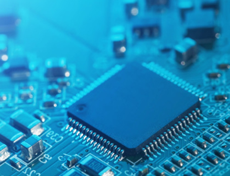
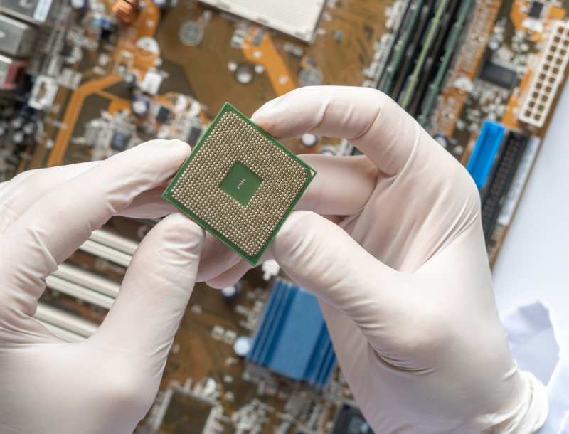
Semiconductor Device Packaging
As semiconductor technologies continue to permeate everything in our daily lives, and become more personal, the devices we use are becoming smaller and more powerful every day. The semiconductor industry has successfully scaled performance and cost through Moore’s Law, but the packaging of semiconductors has not yet approached the same sort of complementary scale due to cost or technology constraints. Increasingly, multiple semiconductor devices must be grouped together to create a single, miniature component module, and semiconductor devices are being stacked to form 3D blocks of circuits. As we move to the era of wearable, printable, and consumable components, packaging must change to be more flexible, organic, digestible, renewable, dissolvable and follow the same integration cost and size advantages as Moore’s Law provides for semiconductor devices.
Research in this area would include advanced materials science research; new materials for flexible or consumable electronics; stacked circuit techniques for advanced integration; packaging substrate manufacturing technology; advanced test techniques for miniature packaging; nano-scale packaging; sustainability or recyclability of packaging materials and manufacturing techniques.
Compound Semiconductor Materials
Compound Semiconductors offer properties & capabilities exceeding those of normal silicon-based devices, enabling improved efficiencies, higher speeds and greater powers in a variety of applications. Arguably the worlds first commercial nanotechnology, LEDs based on Ill-V systems are in a phase of rapid development where there are great industrial needs for lower costs & higher efficiencies. Compound Semiconductors have been used to produce the highest efficiency Solar Cells ever reported and can enable improved RF circuits and more efficient power supplies.
There are opportunities for research in all these areas, and great opportunities to exploit basic Ill-V epitaxy to customise solutions for these emerging applications. Solid State Lasers and customised light sources for sensors in medical/health/wearable markets is a further area where basic compound semiconductor technology can be exploited.
Cheaper Epoxy/Materials for Mass-Market Optoelectronics (MMMO)
Optoelectronic components are appearing in virtually all consumer electronics and many industrial and automotive products, in the near future Opto devices will be the sensors & detectors in wearable devices & autonomous vehicles . The extent of penetration of opto devices is ultimately limited by factors of size & cost.
There are opportunities to research new classes of polymers and develop novel encapsulants, housings & lenses which offer lower costs, greater stabilities, smaller form factors, recyclability etc. In addition there are large industrial demands for low-cost epoxy and silicone systems to meet the needs of consumer electronics – for these ‘mature’ technologies much base IP has expired, creating new opportunities for SME & Start-ups to duplicate & improve materials which are already in high-volume use.